


|
|
slide No. 11 / 12
|
|
|
|
slide No. 11 / 12
Comparisons of the simulation results with experiments are now under way, and here I show an example.
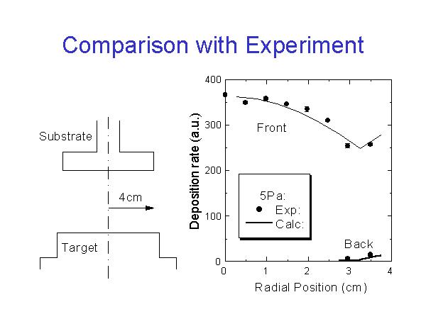
Left is a schematic figure of our deposition chamber, which is modeled with the simulation. It has rotation symmetry, and the substrate radius is 4 cent-meters, and the distance between the target and the substrate is 5 centimeters.
We deposit copper films on glass substrates by DC magnetron sputtering, and measure the film thickness by optical interferometer.
In the Right figure, marks are experimental values, and this line is a calculation result. Horizontal axis is a radius of the measured point, and vertical axis is a normalized deposition rate. It is identical to atomic flux.
The values for front and back faces of the substrate are shown. The agreement is well.
Rates of simulation at back face are slightly smaller, which may be originated from the limitation of the constant approximation we used at BEM calculation. This lead to overestimate the flux at node element near the source point, so the node elements around that node become rather small.
We think that this problem can be solved by using the higher order approximation for the BEM calculation, and the development is also under way.